Description
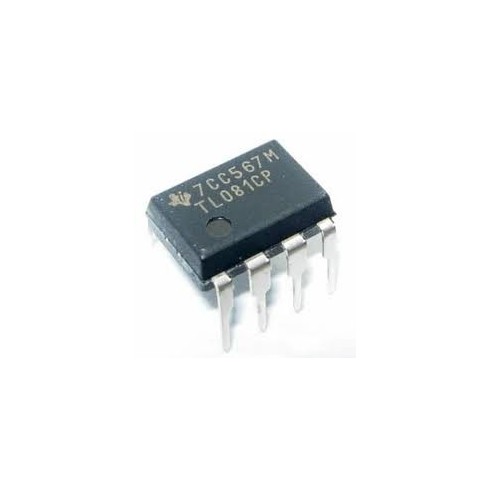
TL081 combines two cutting-edge linear technologies on a single monolithic integrated circuit. Each internally compensated operational amplifier has well-matched high voltage JFET input devices for low input offset voltage. The IC has a range of working conditions a wide range of working voltages and possesses direct interfacing capability with almost every PMOS, CMOS, and NMOS device. Moreover, the IC offers a wide array of features such as high noise immunity, ESD barring/reduction, and exceptionally low power dissipation. TL081 operates over a wide range of commercial, industrial, and military temperature ranges
TL081 Pinout
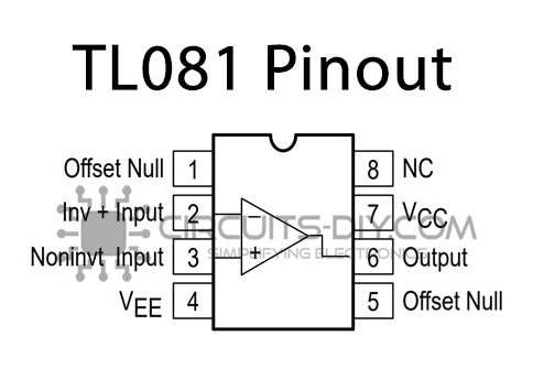
TL081 Pin Configuration
| Pin No | Pin Name | Description |
|---|---|---|
| 1 | OFFSET NULL 1 | Offset Null Pin 1 |
| 2 | INV-INPUT | Inverting Input Of Amplifier |
| 3 | NON-INV-INPUT | Non Inverting Input Of Amplifier |
| 4 | VEE | Emitter Supply Voltage |
| 5 | OFFSET NULL 2 | Offset Null Pin 2 |
| 6 | OUTPUT | Output Of Amplifier |
| 7 | VCC | Collector Supply Voltage |
| 8 | NC | No Connection |
TL081 Features
- Input Offset Voltage Options of 6.0 mV and 15 mV Max
- Low Input Bias Current: 30 pA
- Low Input Offset Current: 5.0 pA
- Wide Gain Bandwidth: 4.0 MHz
- High Slew Rate: 13 V/µs
- Low Supply Current: 1.4 mA per Amplifier
- High Input Impedance: 1012
Application
- Solar energy: string and central inverter
- Motor drives: AC and servo drive control and
- Power stage modules
- Single phase online UPS
- Three phase LIPS
- Pro audio mixers
- Battery test equipment


